Memory for AI Accelerators
AI accelerators are made up of thousands of small circuits (compute units) that do simple math operations. To read input data and store results, they need memory. To make those reads and writes fast, you can use a more expensive memory technology, place it closer to the compute units so the signal travels less distance, or add more wires so more data moves at once. You also want as much memory as possible to fit the billions of numbers that make up modern AI models.
But faster memory is physically larger and more expensive, and there is only so much space on a chip. To balance speed, size, and cost, accelerators use several layers of memory. Smaller, faster, and more expensive memory sits closest to the compute units. Larger, slower, and cheaper memory sits further away.
Why memory is the bottleneck
Processor speed improves faster than memory speed. This is known as the memory wall, coined by Wulf and McKee in 1995 during the CPU era. They predicted processors would eventually spend most of their time waiting on memory rather than computing. [11]Wulf, W. A. & McKee, S. A., "Hitting the Memory Wall: Implications of the Obvious," ACM SIGARCH Computer Architecture News, 23(1), 20–24 (1995)https://dl.acm.org/doi/10.1145/216585.216588 The same thing is now happening to GPUs.
From NVIDIA's V100 in 2017 to the B200 in 2024, HBM bandwidth grew 8.9x, from 900 GB/s to 8 TB/s. Compute throughput grew 18x. The gap widened with every generation. [2]NVIDIA, "NVIDIA B200 Tensor Core GPU" Datasheet (2024)https://www.nvidia.com/en-us/data-center/b200/ [3]NVIDIA, "NVIDIA V100 Tensor Core GPU" Datasheet (2017)https://www.nvidia.com/en-us/data-center/v100/
LLM inference has two phases: prefill (processing the prompt), which is often compute-bound, and decode (token-by-token generation), which is usually memory-bound. Some systems now split prefill and decode onto separate hardware. During decode, each token requires reading model weights and KV-cache data (cached context from previous tokens) while doing a little math per byte fetched, meaning compute units sit idle waiting for data.
The NVIDIA H200 illustrates this. Same Hopper chip as the H100, zero compute changes, only memory bandwidth up 1.4x and capacity increased from 80 GB to 141 GB which resulted in up to 1.9x faster inference for Llama 2 70B. [1]NVIDIA, "NVIDIA H200 Tensor Core GPU" Datasheet (2024)https://www.nvidia.com/en-us/data-center/h200/
The memory hierarchy
There is an important distinction between memory technologies and memory roles. Technologies are different physical ways to store bits. Roles are where data sits in the system and what it does there.
Technologies: how bits are stored
All memory is built from tiny circuits called cells. Each cell stores one bit (a 0 or a 1). The three main technologies differ in how those cells are built, which determines how fast, how large, and how expensive the memory is.
SRAM (static random-access memory) stores each bit using 6 transistors wired in a loop. "Static" means the data stays as long as power is on, no maintenance needed. Fast but physically large and expensive, about $5,000/GB to fabricate.
DRAM (dynamic random-access memory) stores each bit using 1 transistor and 1 tiny capacitor. The capacitor holds a charge, but it leaks within milliseconds. The memory controller must constantly re-read and re-write every bit to keep it alive ("refresh"). 6x less silicon per bit than SRAM makes it far denser and cheaper, but slower. $3-45/GB depending on the variant.
HBM, GDDR, DDR5, and LPDDR, which we will cover later, are all DRAM, meaning they are made up of the thousands of tiny DRAM cells. The difference is packaging and how they connect to the processor.
Flash (NAND) traps charge in an insulated gate that does not leak. Data persists without power (non-volatile). Much slower to write than DRAM, and each write slightly damages the insulator, so cells wear out over time. About $0.10/GB.
| Technology | Transistors per bit | Cell access time (ns, billionths of a second) | Cost per GB |
|---|---|---|---|
| SRAM | 6 | 1-2 ns | ~$5,000 |
| DRAM | 1 + capacitor | 50-100 ns | $3-45 |
| Flash (NAND) | ~1 | 25,000-100,000 ns | ~$0.10 |
Cell access time is how fast a single cell can be read. System-level bandwidth (like HBM's 8 TB/s) is much higher because accelerators read from thousands of cells in parallel through wide buses.
No single technology is simultaneously fast, large, and affordable. SRAM is fast but expensive. DRAM is dense but slow. Flash is cheap but the slowest of the three. This is why accelerators layer them.
Roles: where data sits
These technologies fill different roles depending on the accelerator. Not every chip uses all of them. NVIDIA GPUs have four levels. Groq's LPU has two. The roles are:
Registers sit inside every compute unit and hold the values it is actively working on. Built from transistor circuits similar to SRAM. No address lookup needed: the instruction directly selects which register to read. Extremely fast (1 clock cycle, the smallest unit of time a chip works in) but tiny, only kilobytes per compute unit. Every accelerator has registers.
Caches are built from SRAM. They hold recently used data close to the compute units so it does not have to be fetched from main memory again. Caches come in levels: L1 is the smallest and fastest (a few cycles), private to each compute unit. L2 is larger and shared across multiple units (tens of cycles). On NVIDIA GPUs, caches total tens of megabytes. On Groq and Cerebras, SRAM plays a bigger role: it serves as the chip's main memory (hundreds of megabytes to tens of gigabytes), replacing DRAM entirely.
Main memory is where model weights and activations live during inference. On most GPUs, this is DRAM (HBM or GDDR), providing hundreds of gigabytes with nanosecond-scale latency. On SRAM-only chips like Groq and Cerebras, the on-chip SRAM serves this role instead, with far less capacity but far more bandwidth.
System memory and storage (DDR5 on the host motherboard, SSDs) sit outside the accelerator. Used for loading models at startup, checkpointing, and data that does not fit on the chip. Every accelerator relies on this level, including SRAM-only chips, which load weights from host memory before inference begins.
On a typical GPU, each level is 10-100x larger and 10-100x slower than the one above it. Data moves inward through the hierarchy: storage → system memory → main memory → cache → register → compute unit uses it. Every time data has to come from a further-out level, the compute unit waits.
DDR
DDR (double data rate) is the standard DRAM used on server and desktop motherboards. It is the baseline memory that every computer has. "Double data rate" means it transfers data twice per clock cycle instead of once, doubling bandwidth without increasing the clock speed.
DDR generations roughly double bandwidth each time. DDR4 peaked at about 25 GB/s per channel. DDR5, the current generation, reaches 35-70 GB/s per channel. A typical server has 256-512 GB of DDR5 across multiple channels.
In AI systems, DDR5 sits on the host server motherboard, not on the accelerator itself. It serves as system memory: the CPU uses it for orchestration, data preprocessing, and loading model weights from storage before transferring them to the accelerator. DDR5 costs $3-5/GB, making it the cheapest DRAM option, but its bandwidth is a fraction of what HBM or GDDR can deliver.
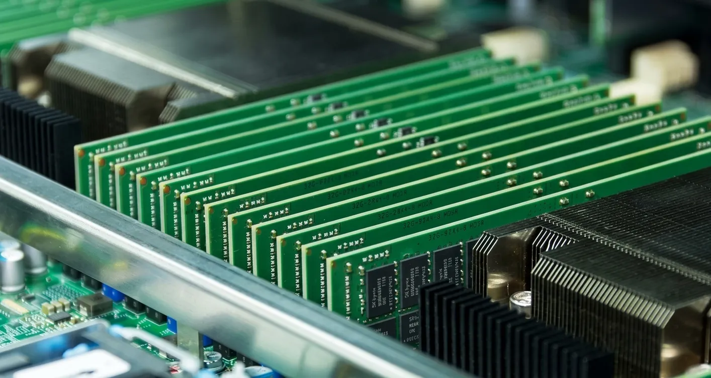
HBM
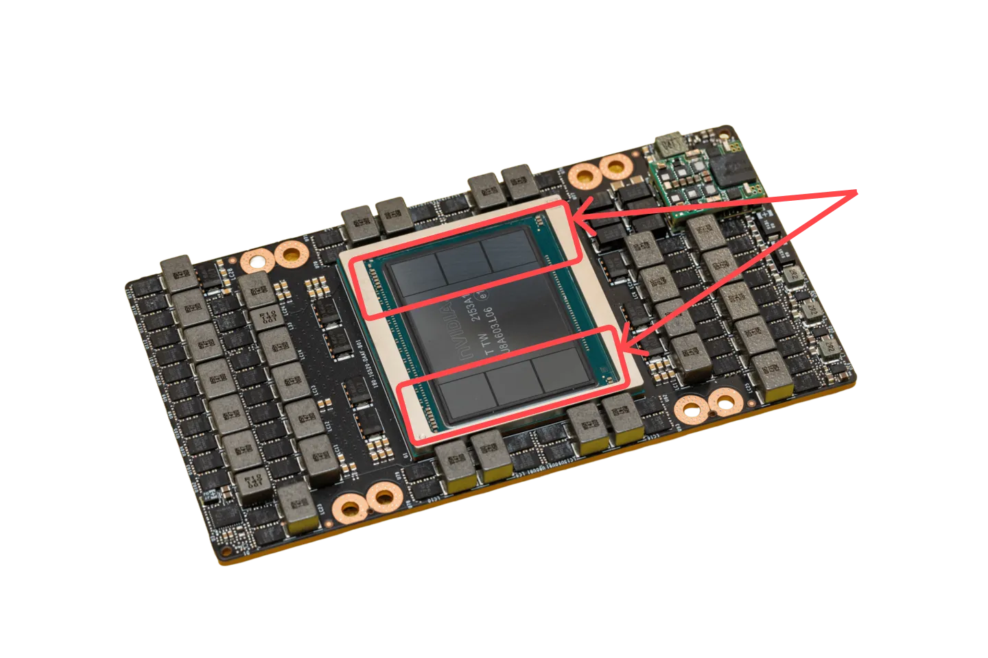
HBM is multiple DRAM chips stacked on top of each other and placed right next to the GPU. Because the memory sits so close it can use thousands of data lines (tiny wires) to talk to the GPU simultaneously, hence the increase in bandwidth. The short data paths also make HBM 2-5x more energy-efficient per bit transferred than DDR5 or GDDR. [6]JEDEC, "High Bandwidth Memory (HBM3)" Standard JESD238A (2022)https://www.jedec.org/standards-documents/docs/jesd238a
| GPU | Year | Memory type | Capacity | Bandwidth |
|---|---|---|---|---|
| V100 | 2017 | HBM2 | 32 GB | 900 GB/s |
| A100 | 2020 | HBM2e | 80 GB | 2.0 TB/s |
| H100 | 2022 | HBM3 | 80 GB | 3.35 TB/s |
| H200 | 2024 | HBM3e | 141 GB | 4.8 TB/s |
| B200 | 2024 | HBM3e | 192 GB | 8 TB/s |
| Rubin (R100, announced) | 2026 | HBM4 | 288 GB | 22 TB/s |
| Rubin Ultra (announced) | 2027 | HBM4E | 1 TB | ~32 TB/s |
From V100 to announced Rubin, bandwidth would grow 24x (900 GB/s to 22 TB/s) and capacity would grow 9x (32 GB to 288 GB). NVIDIA says Rubin will be its first GPU with HBM4, which doubles the interface width to 2,048 bits per stack. [12]Tom's Hardware, "Nvidia's Vera Rubin platform in depth" (March 2026)https://www.tomshardware.com/pc-components/gpus/nvidias-vera-rubin-platform-in-depth-inside-nvidias-most-complex-ai-and-hpc-platform-to-date
HBM capacity determines whether a model fits on one GPU or must be split across several. A 70B-parameter model in FP16 takes roughly 140 GB just for the weights (2 bytes per parameter x 70 billion parameters).
The B200's 192 GB can hold those weights on a single chip. In production you also need room for cached context and runtime overhead, so whether one GPU is enough depends on the workload. The H100's 80 GB is below the weights-only requirement, so the model must be split across two or more GPUs connected via NVLink.
GDDR
Both HBM and GDDR are built from the same DRAM cells. The difference is packaging. GDDR chips are individual DRAM chips soldered onto the circuit board around the GPU, centimeters away, connected by fewer but faster wires.
Fewer wires means less total bandwidth. But GDDR is simpler to manufacture and 3-5x cheaper per GB than HBM. It is the standard memory on consumer GPUs and some inference-oriented data center cards.
Each GDDR generation finds ways to move more data per wire. GDDR6X doubled the data rate by encoding 2 bits per signal instead of 1. GDDR7 pushed the per-pin rate from 21 Gbps to 32 Gbps. [14]Micron, "Doubling I/O Performance with PAM4" GDDR6X Technical Briefhttps://www.micron.com/products/memory/gddr/gddr6x [15]JEDEC, "JEDEC Publishes GDDR7 Graphics Memory Standard" (March 2024)https://www.jedec.org/news/pressreleases/jedec-publishes-gddr7-graphics-memory-standard
NVIDIA used GDDR6X on the RTX 4090 (24 GB, 1 TB/s) and GDDR7 on the RTX 5090 (32 GB, 1.8 TB/s).
GDDR is also expanding into higher-end data center roles. NVIDIA's announced Rubin lineup includes the R100 with HBM4 and a separate chip, the Rubin CPX, with 128 GB of GDDR7.
The CPX targets workloads where the chip is doing enough math per byte that HBM's bandwidth goes underutilized. In those cases, swapping in cheaper GDDR7 lowers memory cost without a meaningful performance penalty. [13]NVIDIA Newsroom, "NVIDIA Unveils Rubin CPX: A New Class of GPU Designed for Massive-Context Inference" (2026)https://nvidianews.nvidia.com/news/nvidia-unveils-rubin-cpx-a-new-class-of-gpu-designed-for-massive-context-inference
SRAM-only accelerators
A few companies have taken a different approach: skip external DRAM entirely and run everything from on-chip SRAM.
Groq's LPU (language processing unit) is the highest-profile example. The chip has no HBM or GDDR attached. All memory is on-chip SRAM. Weights are loaded from host memory at startup and held in SRAM during inference, so the compute units never wait on external memory. [7]Groq, "GroqChip Processor" Architecture Overview (accessed March 2026)https://groq.com/technology/
The first-generation chip had 230 MB of SRAM at 80 TB/s. The latest, the Groq 3 LPU, doubles that to 500 MB at 150 TB/s per chip. [16]Tom's Hardware, "Nvidia Groq 3 LPU and Groq LPX racks join Rubin platform at GTC" (March 2026)https://www.tomshardware.com/pc-components/gpus/nvidia-groq-3-lpu-and-groq-lpx-racks-join-rubin-platform-at-gtc-sram-packed-accelerator-boosts-every-layer-of-the-ai-model-on-every-token
The tradeoff is capacity. 500 MB cannot hold even a small language model. A 7B-parameter model needs roughly 14 GB, so Groq distributes it across dozens of chips. Larger models require hundreds.
In December 2025, Groq and NVIDIA announced a licensing agreement for Groq's inference technology. NVIDIA has since previewed Groq 3 systems alongside the Vera Rubin platform, pairing 256 LPUs (128 GB of SRAM total) with DDR5 for larger models. [17]Groq, "Groq and Nvidia Enter Non-Exclusive Inference Technology Licensing Agreement" (December 2025)https://groq.com/newsroom/groq-and-nvidia-enter-non-exclusive-inference-technology-licensing-agreement-to-accelerate-ai-inference-at-global-scale [16]Tom's Hardware, "Nvidia Groq 3 LPU and Groq LPX racks join Rubin platform at GTC" (March 2026)https://www.tomshardware.com/pc-components/gpus/nvidia-groq-3-lpu-and-groq-lpx-racks-join-rubin-platform-at-gtc-sram-packed-accelerator-boosts-every-layer-of-the-ai-model-on-every-token
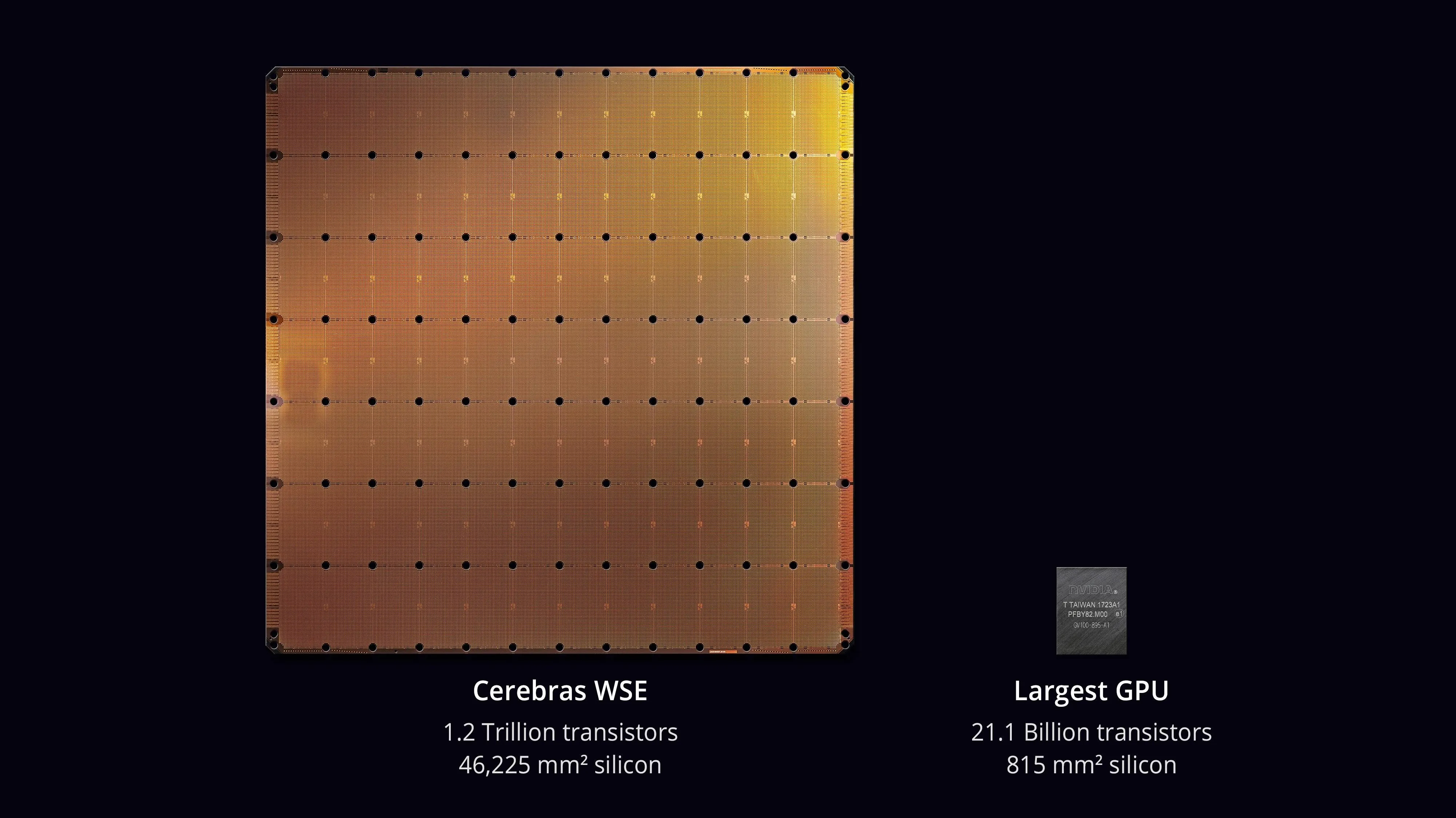
Cerebras took a different approach: build one chip so large it fills an entire silicon wafer. Most chips are cut from wafers in small pieces. Cerebras skips the cutting and uses the whole disc.
The WSE-3 (their third generation) packs 44 GB of SRAM onto that single wafer. Because all the memory is on-chip, data does not have to travel off-chip to reach the compute units. On-chip bandwidth reaches 21 PB/s, roughly 2,600x what a single NVIDIA GPU gets from HBM. [8]Cerebras, "Wafer-Scale Engine 3" Product Page (accessed March 2026)https://cerebras.ai/chip/
For models that exceed 44 GB, Cerebras pairs the wafer with an external system called MemoryX. MemoryX is racks of DRAM and flash that store the full model weights and stream them to the wafer one layer at a time. Configurations range from 12 TB to 1.2 PB. [18]Cerebras, "Announcing the Cerebras Architecture for Extreme-Scale AI" (2024)https://www.cerebras.ai/blog/announcing-the-cerebras-architecture-for-extreme-scale-ai
SRAM at $5,000/GB makes these chips expensive per byte. But the bandwidth per byte is orders of magnitude higher than HBM, which eliminates the memory bottleneck for workloads that fit.
The catch: SRAM-only chips excel at single-request latency but scale poorly with batching. GPUs load each weight from HBM once and multiply it across every request in the batch, so a batch of 64 gets 64x more math per byte loaded. SRAM-only chips are already fast at batch size 1, so batching helps less, and they run out of memory sooner. For high-throughput serving with many simultaneous users, GPUs typically deliver more tokens per dollar.
Memory tradeoffs across accelerators
Every accelerator vendor makes a different bet on memory. The choice signals the target market. The table below mixes shipped products with announced designs where vendors have published memory specs.
| Chip | Memory | Capacity | Bandwidth | |
|---|---|---|---|---|
| HBM | NVIDIA B200 | HBM3e | 192 GB | 8 TB/s |
| AMD MI325X | HBM3e | 256 GB | 6 TB/s | |
| Google TPU v7 | HBM3e | 192 GB | 7.4 TB/s | |
| AWS Trainium3 | HBM3e | 144 GB | 4.9 TB/s | |
| Microsoft Maia 200 | HBM3e | 216 GB | 7 TB/s | |
| Meta MTIA 400 | HBM | 288 GB | 9.2 TB/s | |
| GDDR / LPDDR | NVIDIA Rubin CPX * | GDDR7 | 128 GB | TBD |
| Intel Crescent Island * | LPDDR5X | 160 GB | TBD | |
| SRAM | Groq 3 LPU | SRAM | 500 MB/chip | 150 TB/s |
| Cerebras WSE-3 | SRAM | 44 GB | 21 PB/s | |
| Mixed | SambaNova SN40L | SRAM + HBM + DDR5 | 520 MB + 64 GB + 1.5 TB | 2 TB/s |
* Announced, not yet shipping.
AMD has competed on capacity. The MI325X shipped with 256 GB of HBM3e before NVIDIA shipped anything above 192 GB, making it attractive for large-model inference where weights must fit on a single card. [9]AMD, "AMD Instinct MI300X Accelerator" Datasheet (2023)https://www.amd.com/en/products/accelerators/instinct/mi300/mi300x.html
The hyperscalers are building their own chips to reduce dependence on NVIDIA and the HBM supply chain. Each is only available on its own cloud.
AWS Trainium3 ships with 144 GB of HBM3e at 4.9 TB/s per chip. [20]HPCwire, "AWS Brings the Trainium3 Chip to Market With New EC2 UltraServers" (December 2025)https://www.hpcwire.com/2025/12/02/aws-brings-the-trainium3-chip-to-market-with-new-ec2-ultraservers/ Google's TPU v7 (Ironwood) matches the B200 on capacity at 192 GB and comes close on bandwidth at 7.4 TB/s. [19]Google Cloud, "Inside the Ironwood TPU codesigned AI stack" (April 2025)https://cloud.google.com/blog/products/compute/inside-the-ironwood-tpu-codesigned-ai-stack
Microsoft's Maia 200 ships with 216 GB of HBM3e at 7 TB/s. Optimized for inference on Azure. [21]Microsoft, "Maia 200: The AI accelerator built for inference" (January 2026)https://blogs.microsoft.com/blog/2026/01/26/maia-200-the-ai-accelerator-built-for-inference/
Meta designs its own chips (MTIA) for internal inference. The earlier generations used LPDDR5 (the same type of memory in smartphones) instead of HBM, which limited them to smaller models. The upcoming MTIA 300-500 series switches to HBM, jumping to 216-512 GB per chip. [22]Data Center Dynamics, "Meta unveils next four generations of its MTIA chip" (March 2026)https://www.datacenterdynamics.com/en/news/meta-unveils-next-four-generations-of-its-mtia-chip/
Not everyone is betting on HBM. Tenstorrent uses GDDR6, avoiding HBM's cost and supply constraints. Intel's upcoming Crescent Island uses LPDDR5X, targeting air-cooled enterprise servers where power and cost matter more than peak bandwidth. [23]Tenstorrent, "Blackhole" Product Page (accessed March 2026)https://tenstorrent.com/en/hardware/blackhole [24]Tom's Hardware, "Intel unveils Crescent Island, an inference-only GPU with Xe3P architecture and 160GB of memory" (October 2025)https://www.tomshardware.com/pc-components/gpus/intel-unveils-crescent-island-an-inference-only-gpu-with-xe3p-architecture-and-160gb-of-memory
SambaNova takes a three-tier approach. Its SN40L combines on-chip SRAM, HBM, and DDR5 in a single system: 520 MB + 64 GB + 1.5 TB. This lets it hold trillion-parameter models without distributing across multiple chips. [25]IEEE, "SambaNova SN40L: A 5nm 2.5D Dataflow Accelerator with Three Memory Tiers for Trillion Parameter AI," ISSCC 2025https://ieeexplore.ieee.org/document/10904578/
References
- NVIDIA, "NVIDIA H200 Tensor Core GPU" Datasheet (2024)
- NVIDIA, "NVIDIA B200 Tensor Core GPU" Datasheet (2024)
- NVIDIA, "NVIDIA V100 Tensor Core GPU" Datasheet (2017)
- NVIDIA, "NVIDIA A100 Tensor Core GPU" Datasheet (2020)
- NVIDIA, "NVIDIA H100 Tensor Core GPU" Datasheet (2022)
- JEDEC, "High Bandwidth Memory (HBM3)" Standard JESD238A (2022)
- Groq, "GroqChip Processor" Architecture Overview (accessed March 2026)
- Cerebras, "Wafer-Scale Engine 3" Product Page (accessed March 2026)
- AMD, "AMD Instinct MI300X Accelerator" Datasheet (2023)
- SK Hynix, "HBM3E" Product Page (accessed March 2026)
- Wulf, W. A. & McKee, S. A., "Hitting the Memory Wall: Implications of the Obvious," ACM SIGARCH Computer Architecture News, 23(1), 20–24 (1995)
- Tom's Hardware, "Nvidia's Vera Rubin platform in depth" (March 2026)
- NVIDIA Newsroom, "NVIDIA Unveils Rubin CPX: A New Class of GPU Designed for Massive-Context Inference" (2026)
- Micron, "Doubling I/O Performance with PAM4" GDDR6X Technical Brief
- JEDEC, "JEDEC Publishes GDDR7 Graphics Memory Standard" (March 2024)
- Tom's Hardware, "Nvidia Groq 3 LPU and Groq LPX racks join Rubin platform at GTC" (March 2026)
- Groq, "Groq and Nvidia Enter Non-Exclusive Inference Technology Licensing Agreement" (December 2025)
- Cerebras, "Announcing the Cerebras Architecture for Extreme-Scale AI" (2024)
- Google Cloud, "Inside the Ironwood TPU codesigned AI stack" (April 2025)
- HPCwire, "AWS Brings the Trainium3 Chip to Market With New EC2 UltraServers" (December 2025)
- Microsoft, "Maia 200: The AI accelerator built for inference" (January 2026)
- Data Center Dynamics, "Meta unveils next four generations of its MTIA chip" (March 2026)
- Tenstorrent, "Blackhole" Product Page (accessed March 2026)
- Tom's Hardware, "Intel unveils Crescent Island, an inference-only GPU with Xe3P architecture and 160GB of memory" (October 2025)
- IEEE, "SambaNova SN40L: A 5nm 2.5D Dataflow Accelerator with Three Memory Tiers for Trillion Parameter AI," ISSCC 2025
- TrendForce, "Samsung, SK hynix Reportedly Plan ~20% HBM3E Price Hike for 2026" (December 2025)
- Tom's Hardware, "Here's why HBM is coming for your PC's RAM" (2025)
- Tom's Guide, "Nvidia RTX 50-series GPU production reportedly paused" (2026)
- SemiAnalysis, "Scaling the Memory Wall: The Rise and Roadmap of HBM" (2024)
- Tom's Hardware, "Explosive HBM demand fueling an expected 20% increase in DDR5 memory pricing" (2025)
Frequently Asked Questions
What is HBM and why is it used in AI GPUs?
HBM (high bandwidth memory) is DRAM stacked vertically on the same package as the GPU, connected by thousands of data lanes. A B200 has 192 GB of HBM3e delivering 8 TB/s. AI workloads are memory-bound, compute units process data faster than memory can deliver it, so the wide bus is what keeps tensor cores fed. HBM is also 2-5x more energy-efficient per bit than DDR5 or GDDR.
How much does HBM cost compared to DDR5?
HBM runs $30-45 per GB, roughly 5-10x the cost of DDR5 at $3-5 per GB. The premium comes from stacking 8-12 dies, wiring thousands of vertical connections through each layer, and testing at every stage because a defect in any layer ruins the stack. SRAM, used in on-chip caches and by accelerators like Groq, costs roughly $5,000 per GB.
What is the difference between HBM and GDDR?
Same DRAM cells, different packaging. HBM stacks dies vertically on the GPU package with a 1,024-bit bus (2,048 for HBM4) for high aggregate bandwidth. GDDR sits on the circuit board around the GPU with fewer, faster wires. HBM delivers more total bandwidth and is standard on data center GPUs. GDDR costs 3-5x less per GB and is standard on consumer GPUs. NVIDIA's Rubin CPX brings GDDR7 to the data center for compute-bound prefill workloads.
Why are most AI workloads memory-bound?
Compute throughput has outpaced memory bandwidth by roughly 2x every GPU generation. From V100 to B200, tensor core throughput grew 18x while HBM bandwidth grew 8.9x. LLM token generation (the decode phase) reads model weights and KV-cache data while doing little math per byte fetched. The H200 proved this: same Hopper chip as the H100, only memory upgraded, and Llama 2 70B inference sped up 1.9x.
Who manufactures HBM?
Three companies: SK Hynix (roughly 62% market share as of 2025), Samsung, and Micron. All production capacity is allocated through 2026. The total HBM market is above $50 billion in 2026. Samsung and SK Hynix have both signaled 20% price increases for HBM3e. HBM competes for the same wafer capacity as DDR5, which drove DDR5 consumer prices up 50% in Q4 2025 as fabs reallocated toward HBM.
We help emerging neoclouds find financing partners, and help financing partners enhance story credit with GPU collateral management and residual value insurance solutions.
Learn how it works →